Improvements in Electronics & Semiconductor Manufacturing focus on enhancing production efficiency, reducing costs, advancing technology, and meeting the increasing demand for higher-performance, smaller, and more reliable electronic devices. These improvements are driven by the rapid evolution of semiconductor technology, automation, sustainability, and material innovations. Below are the key categories of improvements in Electronics & Semiconductor Manufacturing:
1. Advanced Manufacturing Technologies
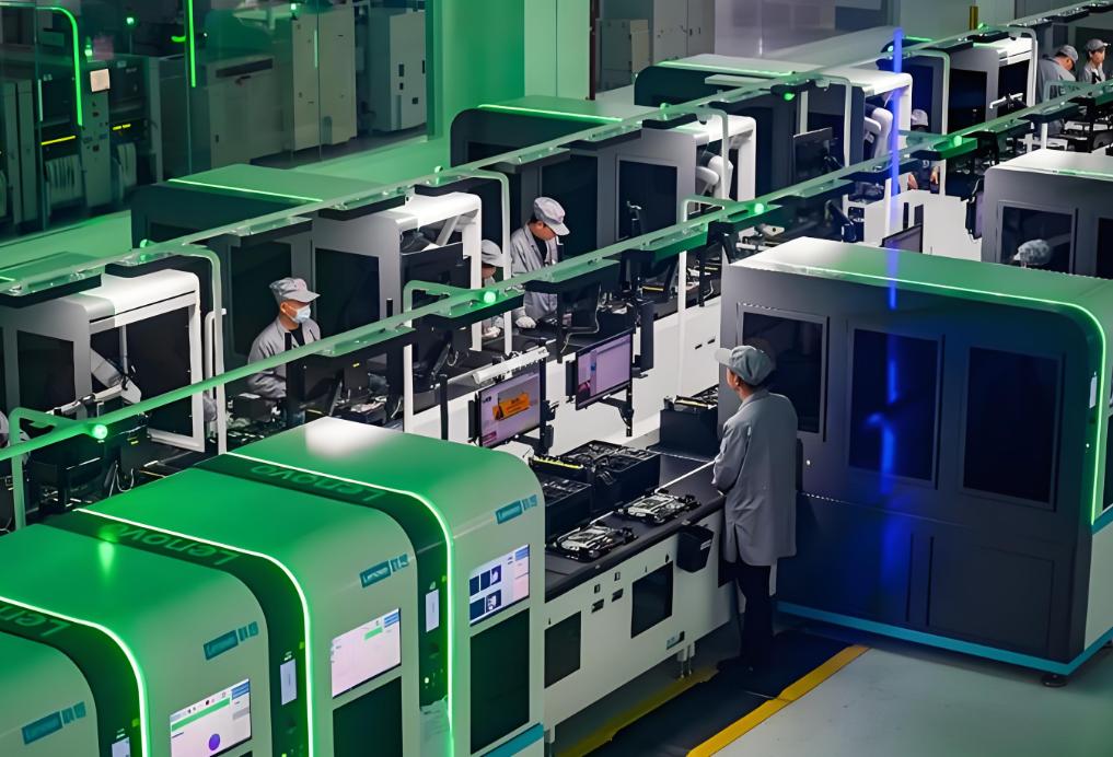
Automation and Robotics: The use of robotic systems and automated production lines to handle repetitive tasks, such as assembly, testing, and packaging, reducing human error, improving efficiency, and cutting down on labor costs.
Advanced Packaging: 3D packaging and system-in-package (SiP) technologies that allow for higher density and integration of semiconductor components, making devices smaller, faster, and more powerful while reducing costs.
Semiconductor Lithography Advances: The development of extreme ultraviolet (EUV) lithography and other advanced photolithographic techniques that enable the production of smaller and more precise semiconductor chips, advancing Moore’s Law (the doubling of transistor density every two years).
Additive Manufacturing (3D Printing): The integration of 3D printing to create complex components and prototypes more efficiently, reducing material waste and allowing for quicker prototyping and product iteration.
2. Material Innovations
New Semiconductor Materials: The exploration and use of wide bandgap materials such as silicon carbide (SiC) and gallium nitride (GaN), which allow for the production of high-power, high-efficiency devices, particularly in the fields of power electronics, 5G, and electric vehicles.
Graphene and 2D Materials: Research into graphene and other 2D materials for future semiconductor applications, offering faster electron mobility, better heat dissipation, and enhanced electrical performance compared to traditional silicon.
Flexible Electronics: The development of flexible semiconductors and stretchable electronics, opening up new possibilities for wearable devices, health-monitoring systems, and smart textiles.
3. Process Optimization and Efficiency
Energy-Efficient Manufacturing: The introduction of energy-efficient processes in semiconductor fabrication, reducing energy consumption and costs in the production of semiconductors, and aligning with sustainability goals.
Yield Improvement: Implementing advanced quality control and statistical process control (SPC) methods to optimize the manufacturing yield, ensuring that a higher percentage of semiconductors pass quality tests and reducing scrap.
Smart Manufacturing Systems: The integration of smart sensors, IoT devices, and machine learning algorithms into production lines for predictive maintenance, real-time quality monitoring, and process optimization.
High-Volume Production: Innovations aimed at increasing the scalability of semiconductor production, such as the use of multi-chamber systems in semiconductor fabrication and advancements in wafer size and handling.
4. Miniaturization and Integration
Smaller Devices: The continued miniaturization of components, including transistors and circuits, allowing for the production of smaller and more powerful electronic devices that can be used in everything from mobile phones to wearable technologies.
System on Chip (SoC) Integration: SoC technologies that integrate multiple components, such as processors, memory, and communication modules, onto a single chip, reducing size, cost, and power consumption.
High-Density Interconnects: Advances in multi-layer PCBs (printed circuit boards), through-silicon vias (TSVs), and interposer-based packaging that enable higher-density interconnects and improved performance in compact devices.
5. Sustainability and Environmental Impact Reduction
Green Electronics Manufacturing: The adoption of eco-friendly manufacturing processes, such as eliminating hazardous chemicals from production, reducing waste, and recycling materials like silicon and metals used in semiconductor devices.
Energy-Efficient Semiconductor Devices: The development of low-power chips for applications such as mobile devices, IoT sensors, and wearable technologies, optimizing energy consumption and extending battery life.
End-of-Life Recycling: Improved methods for recycling semiconductors and electronic waste (e-waste), including the recovery of precious metals (e.g., gold, copper, silver) from old electronics, and the development of biodegradable components.
6. Advanced Testing and Quality Assurance
In-Line Testing: Implementing in-line testing and real-time monitoring of semiconductor devices during the manufacturing process, allowing for early detection of defects and reducing the need for costly post-production quality checks.
Automated Inspection Systems: The use of AI-powered inspection systems that employ machine vision and deep learning algorithms to detect defects in semiconductor wafers or components, enhancing the speed and accuracy of quality control.
Failure Analysis and Reliability Testing: Advanced failure analysis techniques such as scanning electron microscopy (SEM) and X-ray inspection to identify weaknesses in components and ensure the reliability and longevity of semiconductor devices.
7. Semiconductor Fabrication Innovations
Atomic Layer Deposition (ALD): The use of ALD technology for the precise deposition of ultra-thin films on semiconductor wafers, improving the quality and performance of gate oxides, dielectrics, and metals in integrated circuits.
Plasma Etching: Advancements in plasma etching technologies to etch smaller and more intricate patterns on semiconductor wafers, which is essential for the manufacturing of advanced semiconductor nodes (e.g., 7nm, 5nm).
Chemical Vapor Deposition (CVD): The evolution of CVD techniques for the deposition of thin films used in semiconductor manufacturing, allowing for better control over the composition and thickness of deposited materials, which is critical for the miniaturization of devices.
8. 5G and Next-Generation Communication
5G Semiconductor Solutions: Innovations in semiconductor manufacturing to meet the demands of 5G technology, focusing on chips that support higher speeds, greater bandwidth, and lower latency. These improvements include millimeter-wave transistors, RF components, and advanced power amplifiers.
Low-Latency Chips: Development of low-latency semiconductors for real-time data processing applications such as autonomous vehicles, IoT, smart cities, and remote healthcare.
Advanced Connectivity Chips: The design and manufacturing of high-performance connectivity chips, such as Wi-Fi 6, Bluetooth 5.0, and 5G modems, supporting seamless and high-speed data communication in various consumer and industrial devices.
9. Advanced Semiconductor Nodes and Process Technology
Smaller Process Nodes: The reduction of process node sizes (e.g., 7nm, 5nm, 3nm) in semiconductor manufacturing to increase transistor density, speed, and power efficiency while reducing device size.
FinFET and Gate-All-Around (GAA) Transistors: The adoption of advanced transistor architectures like FinFET and GAA to improve performance, energy efficiency, and scalability at smaller nodes.
Quantum Dots and Nanoelectronics: The exploration of quantum dots and nanoelectronics to develop even smaller and more efficient transistors, potentially offering breakthroughs in computing and data storage.
10. Supply Chain and Logistics Optimization
Digital Supply Chain Integration: The use of AI, blockchain, and IoT to streamline the supply chain management process, reduce costs, and improve traceability and transparency of materials used in semiconductor production.
On-Demand Manufacturing: The rise of on-demand semiconductor manufacturing with agile production systems that allow for customized designs and shorter lead times, improving the ability to adapt to market changes and customer needs.
Risk Management: Enhancing supply chain risk management to prevent disruptions due to global shortages (e.g., chip shortages), using predictive analytics, and creating diverse sourcing strategies for critical materials and components.
11. Cybersecurity and Data Privacy
Secure Semiconductor Designs: The incorporation of hardware-level security into semiconductor chips to defend against cyberattacks, ensuring the integrity of data and preventing hacking attempts on devices such as smartphones, IoT devices, and data centers.
Secure Communication Chips: Development of secure communication semiconductors, such as cryptographic processors and encryption chips, that ensure data privacy and safeguard sensitive information transmitted across devices.
12. Artificial Intelligence and Machine Learning Integration
AI-Optimized Semiconductors: The development of specialized AI chips and neural processing units (NPUs) that accelerate machine learning tasks and support edge computing for real-time data processing in IoT devices, autonomous systems, and robotics.
Machine Learning for Design Optimization: Using machine learning algorithms to optimize semiconductor design, improving performance, power efficiency, and cost-effectiveness of chips at each manufacturing stage.
Improvements in Electronics & Semiconductor Manufacturing focus on enhancing production efficiency, reducing costs, advancing technology, and meeting the increasing demand for higher-performance, smaller, and more reliable electronic devices. These improvements are driven by the rapid evolution of semiconductor technology, automation, sustainability, and material innovations. Below are the key categories of improvements in Electronics & Semiconductor Manufacturing:
1. Advanced Manufacturing Technologies
Automation and Robotics: The use of robotic systems and automated production lines to handle repetitive tasks, such as assembly, testing, and packaging, reducing human error, improving efficiency, and cutting down on labor costs.
Advanced Packaging: 3D packaging and system-in-package (SiP) technologies that allow for higher density and integration of semiconductor components, making devices smaller, faster, and more powerful while reducing costs.
Semiconductor Lithography Advances: The development of extreme ultraviolet (EUV) lithography and other advanced photolithographic techniques that enable the production of smaller and more precise semiconductor chips, advancing Moore’s Law (the doubling of transistor density every two years).
Additive Manufacturing (3D Printing): The integration of 3D printing to create complex components and prototypes more efficiently, reducing material waste and allowing for quicker prototyping and product iteration.
2. Material Innovations
New Semiconductor Materials: The exploration and use of wide bandgap materials such as silicon carbide (SiC) and gallium nitride (GaN), which allow for the production of high-power, high-efficiency devices, particularly in the fields of power electronics, 5G, and electric vehicles.
Graphene and 2D Materials: Research into graphene and other 2D materials for future semiconductor applications, offering faster electron mobility, better heat dissipation, and enhanced electrical performance compared to traditional silicon.
Flexible Electronics: The development of flexible semiconductors and stretchable electronics, opening up new possibilities for wearable devices, health-monitoring systems, and smart textiles.
3. Process Optimization and Efficiency
Energy-Efficient Manufacturing: The introduction of energy-efficient processes in semiconductor fabrication, reducing energy consumption and costs in the production of semiconductors, and aligning with sustainability goals.
Yield Improvement: Implementing advanced quality control and statistical process control (SPC) methods to optimize the manufacturing yield, ensuring that a higher percentage of semiconductors pass quality tests and reducing scrap.
Smart Manufacturing Systems: The integration of smart sensors, IoT devices, and machine learning algorithms into production lines for predictive maintenance, real-time quality monitoring, and process optimization.
High-Volume Production: Innovations aimed at increasing the scalability of semiconductor production, such as the use of multi-chamber systems in semiconductor fabrication and advancements in wafer size and handling.
4. Miniaturization and Integration
Smaller Devices: The continued miniaturization of components, including transistors and circuits, allowing for the production of smaller and more powerful electronic devices that can be used in everything from mobile phones to wearable technologies.
System on Chip (SoC) Integration: SoC technologies that integrate multiple components, such as processors, memory, and communication modules, onto a single chip, reducing size, cost, and power consumption.
High-Density Interconnects: Advances in multi-layer PCBs (printed circuit boards), through-silicon vias (TSVs), and interposer-based packaging that enable higher-density interconnects and improved performance in compact devices.
5. Sustainability and Environmental Impact Reduction
Green Electronics Manufacturing: The adoption of eco-friendly manufacturing processes, such as eliminating hazardous chemicals from production, reducing waste, and recycling materials like silicon and metals used in semiconductor devices.
Energy-Efficient Semiconductor Devices: The development of low-power chips for applications such as mobile devices, IoT sensors, and wearable technologies, optimizing energy consumption and extending battery life.
End-of-Life Recycling: Improved methods for recycling semiconductors and electronic waste (e-waste), including the recovery of precious metals (e.g., gold, copper, silver) from old electronics, and the development of biodegradable components.
6. Advanced Testing and Quality Assurance
In-Line Testing: Implementing in-line testing and real-time monitoring of semiconductor devices during the manufacturing process, allowing for early detection of defects and reducing the need for costly post-production quality checks.
Automated Inspection Systems: The use of AI-powered inspection systems that employ machine vision and deep learning algorithms to detect defects in semiconductor wafers or components, enhancing the speed and accuracy of quality control.
Failure Analysis and Reliability Testing: Advanced failure analysis techniques such as scanning electron microscopy (SEM) and X-ray inspection to identify weaknesses in components and ensure the reliability and longevity of semiconductor devices.
7. Semiconductor Fabrication Innovations
Atomic Layer Deposition (ALD): The use of ALD technology for the precise deposition of ultra-thin films on semiconductor wafers, improving the quality and performance of gate oxides, dielectrics, and metals in integrated circuits.
Plasma Etching: Advancements in plasma etching technologies to etch smaller and more intricate patterns on semiconductor wafers, which is essential for the manufacturing of advanced semiconductor nodes (e.g., 7nm, 5nm).
Chemical Vapor Deposition (CVD): The evolution of CVD techniques for the deposition of thin films used in semiconductor manufacturing, allowing for better control over the composition and thickness of deposited materials, which is critical for the miniaturization of devices.
8. 5G and Next-Generation Communication
5G Semiconductor Solutions: Innovations in semiconductor manufacturing to meet the demands of 5G technology, focusing on chips that support higher speeds, greater bandwidth, and lower latency. These improvements include millimeter-wave transistors, RF components, and advanced power amplifiers.
Low-Latency Chips: Development of low-latency semiconductors for real-time data processing applications such as autonomous vehicles, IoT, smart cities, and remote healthcare.
Advanced Connectivity Chips: The design and manufacturing of high-performance connectivity chips, such as Wi-Fi 6, Bluetooth 5.0, and 5G modems, supporting seamless and high-speed data communication in various consumer and industrial devices.
9. Advanced Semiconductor Nodes and Process Technology
Smaller Process Nodes: The reduction of process node sizes (e.g., 7nm, 5nm, 3nm) in semiconductor manufacturing to increase transistor density, speed, and power efficiency while reducing device size.
FinFET and Gate-All-Around (GAA) Transistors: The adoption of advanced transistor architectures like FinFET and GAA to improve performance, energy efficiency, and scalability at smaller nodes.
Quantum Dots and Nanoelectronics: The exploration of quantum dots and nanoelectronics to develop even smaller and more efficient transistors, potentially offering breakthroughs in computing and data storage.
10. Supply Chain and Logistics Optimization
Digital Supply Chain Integration: The use of AI, blockchain, and IoT to streamline the supply chain management process, reduce costs, and improve traceability and transparency of materials used in semiconductor production.
On-Demand Manufacturing: The rise of on-demand semiconductor manufacturing with agile production systems that allow for customized designs and shorter lead times, improving the ability to adapt to market changes and customer needs.
Risk Management: Enhancing supply chain risk management to prevent disruptions due to global shortages (e.g., chip shortages), using predictive analytics, and creating diverse sourcing strategies for critical materials and components.
11. Cybersecurity and Data Privacy
Secure Semiconductor Designs: The incorporation of hardware-level security into semiconductor chips to defend against cyberattacks, ensuring the integrity of data and preventing hacking attempts on devices such as smartphones, IoT devices, and data centers.
Secure Communication Chips: Development of secure communication semiconductors, such as cryptographic processors and encryption chips, that ensure data privacy and safeguard sensitive information transmitted across devices.
12. Artificial Intelligence and Machine Learning Integration
AI-Optimized Semiconductors: The development of specialized AI chips and neural processing units (NPUs) that accelerate machine learning tasks and support edge computing for real-time data processing in IoT devices, autonomous systems, and robotics.
Machine Learning for Design Optimization: Using machine learning algorithms to optimize semiconductor design, improving performance, power efficiency, and cost-effectiveness of chips at each manufacturing stage.
[ Retract  ]
]


 地址
地址 


